


It is reported that Intel CEO Pat Gelsinger met with several senior executives from Korean companies last year to brief them on the latest updates regarding Intel’s foundry business plans.
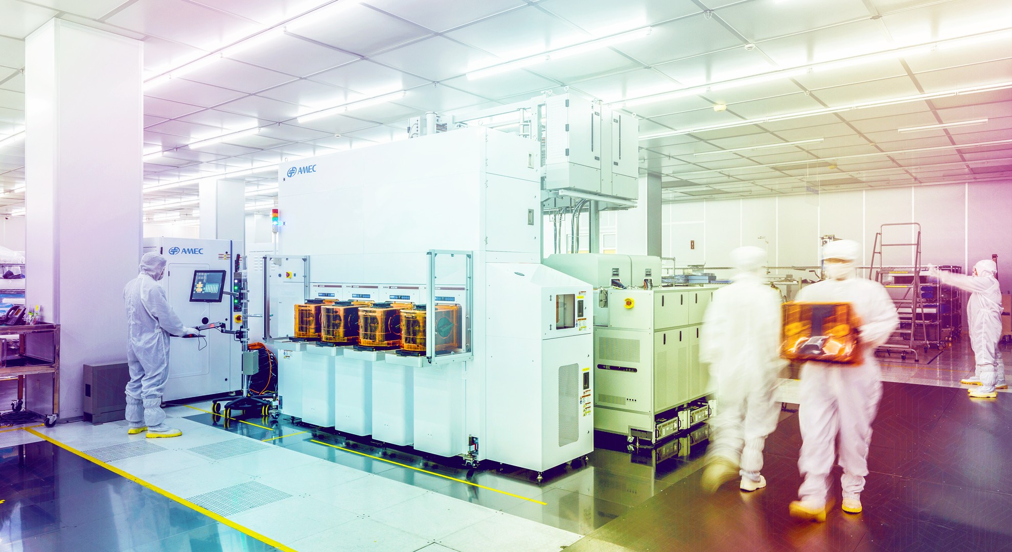
The report states that Intel is aggressively promoting its 18A process node to Korean chip startups and is offering various incentives to encourage adoption.
On Wednesday, Intel released its roadmap for the 14A process node (equivalent to 1.4 nanometers) and announced that chips manufactured using this technology will enter mass production in 2027. The company also revealed that it has secured orders worth $15 billion (currently equivalent to approximately RMB 108 billion) so far.
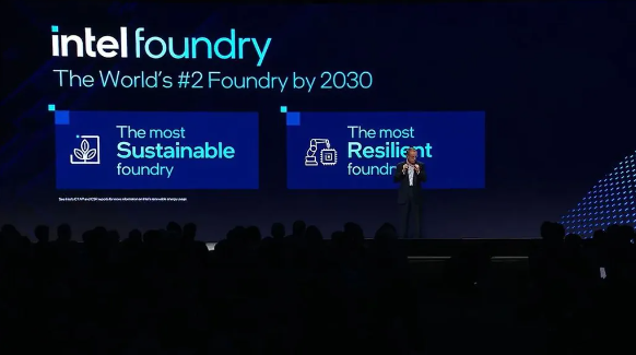
Intel reiterated its goal of becoming the second-largest foundry by 2030, aiming to surpass Samsung, the current runner-up, and trailing only market leader TSMC.
According to Intel, volume production of its 18A process technology will commence by the end of this year, potentially giving the company a lead over its foundry competitors Samsung and TSMC in terms of process technology development. Samsung plans to adopt a gate-all-around (GAA) structure for its 3nm process before transitioning to a 2nm process. Meanwhile, both TSMC and Intel are opting for a FinFET structure for their 3nm chips.
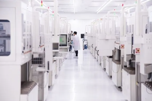
February 27, 2024 – According to a report by South Korean media outlet The Elec, Intel has significantly ramped up its marketing efforts towards Korean fabless chip companies to promote its Intel 18A process technology.
It is reported that Intel CEO Pat Gelsinger met with several senior executives from Korean companies last year to brief them on the latest updates regarding Intel’s foundry business plans.
The report states that Intel is aggressively promoting its 18A process node to Korean chip startups and is offering various incentives to encourage adoption.
On Wednesday, Intel released its roadmap for the 14A process node (equivalent to 1.4 nanometers) and announced that chips manufactured using this technology will enter mass production in 2027. The company also revealed that it has secured orders worth $15 billion (currently equivalent to approximately RMB 108 billion) so far.
Intel reiterated its goal of becoming the second-largest foundry by 2030, aiming to surpass Samsung, the current runner-up, and trailing only market leader TSMC.
According to Intel, volume production of its 18A process technology will commence by the end of this year, potentially giving the company a lead over its foundry competitors Samsung and TSMC in terms of process technology development. Samsung plans to adopt a gate-all-around (GAA) structure for its 3nm process before transitioning to a 2nm process. Meanwhile, both TSMC and Intel are opting for a FinFET structure for their 3nm chips.