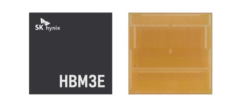
February 27, 2024 – Samsung Electronics announced today that it has successfully developed the industry’s first 36GB 12H (12-layer stacked) HBM3E DRAM, solidifying its leadership position in the high-capacity HBM market.
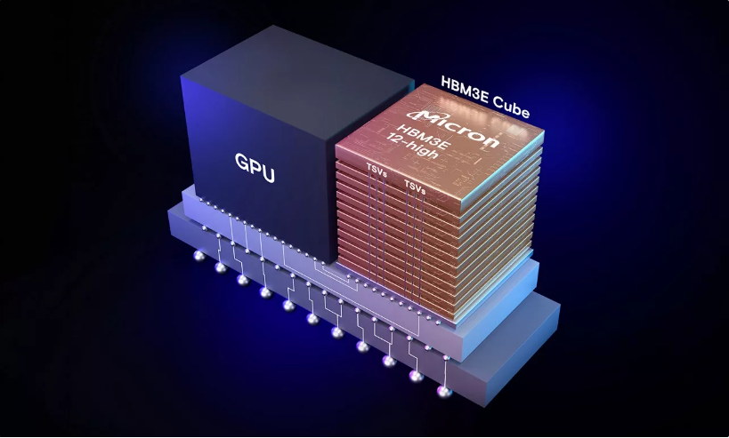
Utilizing TSV (Through Silicon Via) technology, Samsung achieved the industry’s largest 36GB HBM3E 12H capacity by stacking 24Gb DRAM chips to 12 layers. This innovation offers a significant advancement in memory technology.
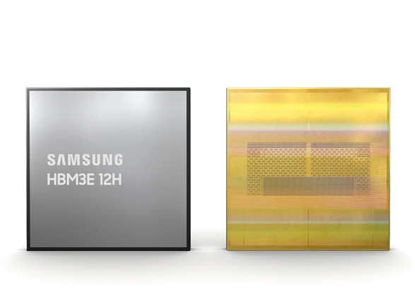
The HBM3E 12H provides an impressive bandwidth of up to 1280GB/s and a maximum capacity of 36GB, representing an increase of over 50% in both bandwidth and capacity compared to its predecessor, the 8-layer stacked HBM3 8H.
Notably, Samsung has maintained the same height for the 12H product as the 8H product through the use of advanced TC NCF (Thermal Compression Non-Conductive Film) technology, ensuring compatibility with HBM packaging specifications.
The application of this cutting-edge TC NCF technology not only increases the number of HBM stacks but also minimizes the “warpage phenomenon” that can occur due to chip thinning, facilitating high-end stacking expansion.
Furthermore, Samsung has continually reduced the thickness of NCF materials, achieving an industry-leading chip spacing of just 7 microns and enabling over 20% higher vertical integration compared to HBM3 8H.
Samsung stated that the HBM3E 12H is poised to become the optimal solution for companies utilizing AI platforms. Compared to HBM3 8H, it offers an average improvement of 34% in AI training speed and can accommodate over 11.5 times more users for inference services.
Currently, Samsung Electronics has begun providing HBM3E 12H samples to customers and anticipates mass production in the first half of this year.

