





August 6, 2026 – In a rare public appearance, Liao Heng, Huawei’s Chief Semiconductor Scientist, issued a stark warning to the global tech industry: leading chipmakers, including NVIDIA, are rapidly approaching an unavoidable physical limit in their pursuit of ever-greater processing power.
Liao pointed out that the decades-old semiconductor strategy of continuously shrinking transistor sizes to pack higher densities onto a single die is nearing its end. NVIDIA, currently the dominant force in AI chips, has been relying on scaling up chip dimensions and stacking an increasing number of High Bandwidth Memory (HBM) modules to trade raw size for performance. However, Liao cautioned that this approach of expanding chip area and memory capacity has a definitive ceiling. Once the industry hits this physical boundary, the entire semiconductor sector could face an “avalanche-like” stagnation.
His remarks echo a long-standing industry consensus that foundries like TSMC and Intel will eventually hit an insurmountable bottleneck in shrinking individual transistors. Historically, these manufacturers have relied on ASML’s indispensable Extreme Ultraviolet (EUV) lithography equipment to advance their roadmaps. However, due to export restrictions preventing Huawei from acquiring these top-tier tools, the Chinese tech giant was forced to forge an alternative path that does not depend on traditional geometric scaling.
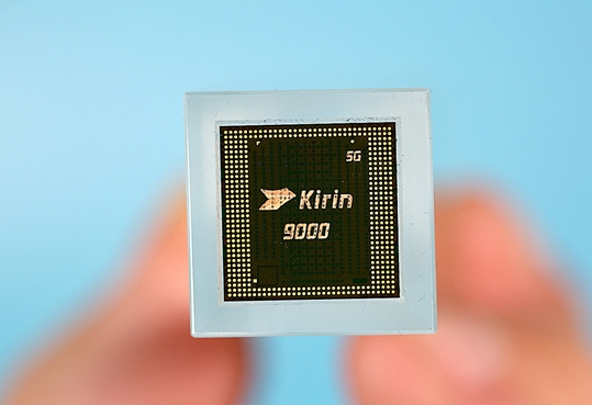
The result is Huawei’s newly proposed “Tau (τ) Law,” which shifts the focus from shrinking physical dimensions to maximizing signal transmission speed across computer systems. As the traditional performance dividends of Moore’s Law diminish, the Tau Law aims to establish a completely new growth curve. Central to this paradigm is a proprietary technology called Logic Folding, which will debut in Huawei’s upcoming smartphone chip.
Unlike conventional 3D chip stacking, which simply layers multiple chips on top of each other, Logic Folding fundamentally restructures the internal circuit layout. By drastically shortening the critical paths for signal transmission, this approach reduces both the time and energy consumed during data transfer. Consequently, actual performance and equivalent transistor density can be significantly boosted without relying on the most advanced, cutting-edge manufacturing nodes.
The scope of the Tau Law extends far beyond a single chip. According to Huawei, this optimization framework spans the entire computing ecosystem—from foundational device physics and circuit design to chip architecture and distributed system interconnects. The ultimate goal is to eliminate wasted time caused by inefficient transmission, redundant communication, and idle waiting across the entire computational workflow.
Far from being a theoretical concept, the Tau Law has already been rigorously tested in production. Huawei disclosed that over the past six years, it has successfully designed and mass-produced 381 commercial chips utilizing this new technical framework, proving that there is indeed a viable alternative route for China’s semiconductor industry to navigate the post-Moore era.