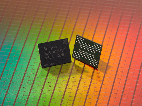
**August 9, 2023 -** In a significant stride towards technological advancement, SK Hynix has revealed its pioneering work in the realm of NAND flash memory. Breaking new ground, the company has unveiled a prototype of 321-layer 1Tb TLC NAND, cementing its position as the pioneer in developing NAND flash memory with over 300 layers.
The unveiling of the 321-layer 1Tb TLC NAND marks a remarkable leap in efficiency, outshining its predecessor, the 238-layer 512Gb NAND, by an impressive 59%. This stride in efficiency is attributed to the ingenious stacking of data storage units, facilitating greater storage capacity within the same chip and subsequently elevating the output per wafer.

As part of its commitment to innovation, SK Hynix is not solely focusing on current accomplishments but is actively steering towards the future. The company plans to commence mass production of the 321-layer NAND in the first half of 2025, underlining its dedication to maintaining technological leadership.
The ascent doesn’t stop there. SK Hynix has extended its technological prowess to the development of next-generation NAND product solutions. These solutions encompass Enterprise SSDs (eSSDs) with PCIe 5 (Gen5) interfaces, catering to the burgeoning demands of the market. Additionally, the company introduces UFS 4.0, a versatile and optimized solution that promises enhanced performance and efficiency.
Moreover, SK Hynix’s trajectory remains forward-looking. Building upon their accumulated product technology and ongoing refinement of in-house solutions, they’re actively engaged in the development of PCI 6.0 and UFS 5.0 products. This resolute commitment underscores their aspiration to maintain a trailblazing role in shaping the future of the market.


