March 04, 2024 – According to recent reports from TheElec, Samsung is considering the application of Molded Underfill (MUF) technology in its next-generation DRAM. The company has recently tested an MR MUF process for 3D-stacked (3DS) memory, which showed improved throughput compared to Thermal Compression Non-Conductive Film (TC NCF) but experienced some deterioration in physical characteristics.
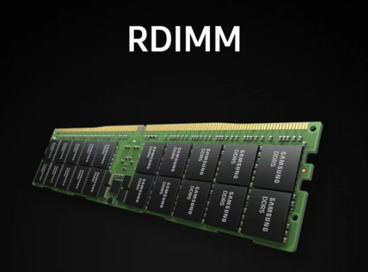
After conducting tests, Samsung concluded that MUF is not suitable for High Bandwidth Memory (HBM) but is well-suited for 3DS RDIMM, currently manufactured using Through-Silicon Via (TSV) technology and primarily used in servers.
MUF is a material injected between semiconductors after the TSV process, which involves drilling thousands of microscopic holes in the semiconductors to connect the upper and lower layers. Its function is to securely fix and connect multiple vertically stacked semiconductors.
Prior to this, Samsung had already employed TC NCF technology in its existing Registered Dual In-line Memory Modules (RDIMM). Meanwhile, MUF is a technology utilized by SK Hynix in the manufacturing of HBM, specifically known as Mass Re-flow Molded Underfill (MR-MUF).
Investigations reveal that MUF, an epoxy resin mold compound, has gained increasing attention in the chip industry following SK Hynix’s successful application in HBM production. The material is believed to have advantages in avoiding wafer warpage.
According to sources, the compound used by SK Hynix was developed in collaboration with Namics. However, Samsung plans to develop its own MUF compound in partnership with Samsung SDI and has already placed orders for the molding equipment required for MUF application.
As the world’s largest semiconductor storage company, Samsung’s potential adoption of MUF could establish it as a mainstream technology and significantly impact the semiconductor material market. Nonetheless, Samsung Electronics officials have responded by stating that they “cannot confirm internal technology strategies.”

