September 12, 2023 – In a rapidly evolving tech landscape, two South Korean giants, Samsung Electronics and SK Hynix, are racing ahead to ramp up production of 12-layer High Bandwidth Memory (HBM). The surging popularity of Generative AI isn’t just driving demand for NVIDIA graphics cards; it’s also fueling the need for high-capacity memory solutions. With each additional layer in HBM stacking, comes increased data processing prowess. Presently, 8-layer HBM stacking reigns supreme, but the next generation with 12 layers is poised for mass production.
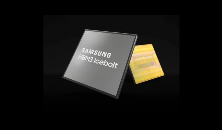
According to reports, the current HBM stacking primarily relies on technologies like Thermal Compression Bonding (TCB) and Mass Reflow (MR) processes. However, the latest buzz suggests that Samsung and SK Hynix are advancing a packaging technique called “Hybrid Bonding,” aiming to shatter the constraints associated with TCB and MR, including thermal issues and packaging height limitations.
The “Hybrid” in Hybrid Bonding refers to more than just copper bumps bonding at room temperature; it entails facing non-conductive parts of two chips squarely together. Consequently, Hybrid Bonding eliminates any gaps between chip-to-chip or wafer-to-wafer connections, eliminating the need for epoxy resin filling.
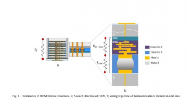
Citing media reports, major players like Samsung Electronics and SK Hynix have overcome these challenges, extending the capabilities of TCB and MR processes to achieve a remarkable 12-layer configuration.
With the adoption of Hybrid Bonding, it’s reported that Input/Output (IO) throughput sees a significant boost, allowing for the connection of 10,000 to 100,000 vias within a 1 square millimeter area. This innovation promises to unlock new frontiers in high-performance computing and data processing, opening up exciting possibilities for next-generation electronics.

