


March 10, 2024 – Samsung Display announced today that it has commenced the construction of a new 8.6-generation IT Organic Light-Emitting Diode (OLED) production line, marking a strategic move to solidify its leadership in the global flat-panel display market.
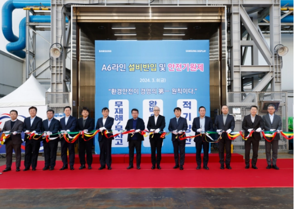
As part of the plan, Samsung Display will transform its existing L8 production line at the central plant in Asan into the A6 production line, dedicated to producing 8.6-generation OLED panels for IT devices beyond smartphones. This will be Samsung Display’s sixth OLED production line, with the installation of major equipment scheduled for this year and mass production set to commence in 2026.
The term “8.6 generation” refers to the size of the substrate used in the production process. A larger substrate allows for the manufacture of larger screens or more smaller screens from a single process, catering to the demand for large screens or significantly improving production efficiency.
In November last year, domestic manufacturer BOE announced plans to invest in the construction of its first 8.6-generation AMOLED production line project in Chengdu, Sichuan Province, China. This marks the country’s inaugural 8.6-generation AMOLED production line.
According to official disclosures, the BOE project spans over an area of 925,200 square meters (approximately 1,388 acres) with a total investment of 63 billion yuan. The registered capital of the project company stands at 38 billion yuan. Specifically, BOE has raised 19.9994 billion yuan, while Chongchan Phase I and the electronics company have each contributed 9.0003 billion yuan. The difference between the total investment and registered capital will be funded through external financing arranged by the project company.
The G8.6 production line (with a glass substrate size of 2,290mm x 2,620mm) being constructed by BOE is based on the existing G6 (glass substrate size of 1,500mm x 1,850mm) OLED production line technology. It aims to further enhance the backlight and OLED light-emitting device manufacturing processes, resulting in products with lower power consumption and longer lifespans compared to previous generations. Additionally, due to the larger substrate size, the slicing efficiency will be higher, leading to reduced production costs.