


January 25, 2024 – In a significant announcement today, Intel revealed that it has achieved mass production utilizing industry-leading semiconductor packaging solutions, highlighting its groundbreaking 3D packaging technology known as Foveros.
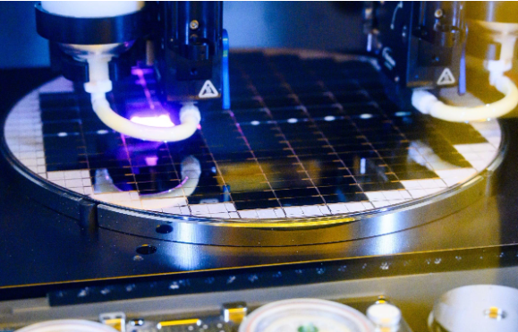
This technological milestone was reached at Intel’s newly upgraded Fab 9 facility in New Mexico, USA. Keyvan Esfarjani, Executive Vice President and Chief Global Operations Officer at Intel, stated, “Advanced packaging technologies like Foveros differentiate Intel and enable our customers to gain a competitive edge in chip performance, form factor, and design flexibility.”
As the semiconductor industry transitions into an era of heterogeneity, where multiple chiplets are integrated into a single package, Intel’s advanced packaging technologies, including Foveros and EMIB (Embedded Multi-die Interconnect Bridge), are poised to revolutionize the industry. These technologies are expected to facilitate the integration of up to one trillion transistors in a single package, thus extending the Moore’s Law beyond 2030.
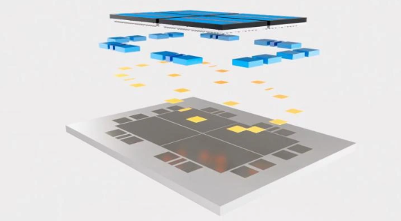
Foveros, Intel’s 3D advanced packaging technology, allows for the vertical stacking of computing modules rather than the traditional horizontal approach during processor manufacturing. This innovation enables Intel and its foundry customers to integrate diverse computing chips, optimizing both cost and energy efficiency.
Previously, the company had announced plans to quadruple its production capacity for 3D Foveros packaging by 2025, indicating a significant ramp-up in its manufacturing capabilities.