July 03, 2024 – In a significant shift from its traditional reliance on Sony for CMOS Image Sensors (CIS), Apple is reportedly advancing plans to diversify its supply chain by incorporating Samsung Electronics as a secondary supplier. According to sources cited by TheElec, Samsung’s System LSI division is currently undergoing final quality assessments for its CIS technology, destined for the primary camera of Apple’s upcoming iPhone generation.
This strategic move follows a tumultuous period in Apple’s partnership with Sony, where supply delays last year hindered the timely launch of the iPhone 15. In response, Apple reportedly tasked Samsung with developing CIS solutions to mitigate future supply chain vulnerabilities and foster competition within the market.
Industry insiders contend that should Samsung successfully pass these rigorous quality tests – a likelihood deemed high by several observers – it would mark a historic milestone for the Korean tech giant, as it would be the first time it supplies CIS to Apple, thereby ending Sony’s long-standing monopoly in this domain.
“This project is tailored to meet Apple’s stringent demands, and if Samsung passes the tests, supply issues should no longer be a concern,” remarked one industry expert. “While Sony will undoubtedly remain a cornerstone supplier, Samsung stands poised to significantly expand its market share.”
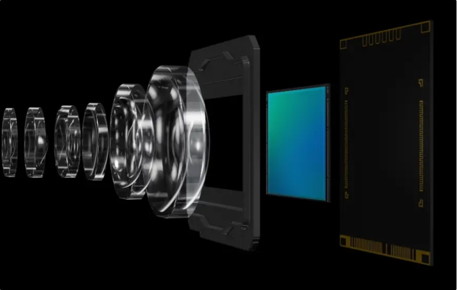
Moreover, TheElec highlights that the novel CIS featured in the iPhone 16 will harness Samsung’s cutting-edge triple-wafer stacking technology. This innovative approach layers three distinct wafers, integrating photodiodes, transistors, and the logic section of analog-to-digital converters. In contrast, previous generations relied on a dual-stack design (marketed by Sony as “Double Transistor Pixel Stacked CMOS Image Sensor Technology”), which combined photodiodes and transistor layers.
The triple-wafer stacking design facilitates electrical interconnection between layers, offering a marked improvement over conventional dual-stack technology. This three-dimensional integration at the wafer level enhances transmission speeds, minimizes latency, and results in superior performance coupled with reduced power consumption.
To elucidate, CIS functionality necessitates the synergy between a photodiode and four transistors. The photodiode is responsible for converting light signals into electrical signals, while the transistors facilitate their transmission, amplification, readout, and erasure. Apple and other industry leaders emphasize the necessity of segregating photodiodes and transistors, which necessitates wafer separation, individual processing, and a hybrid stacking methodology to unite the three logical wafers. This approach enables Apple to achieve higher pixel densities (by shrinking pixel sizes) while significantly reducing noise levels through minimized interference.
Crucially, this stacking technology dispenses with the need for signal transmission bumps, instead relying on direct copper pad connections. This design refinement not only reduces the size of the CIS but also accelerates data transmission rates between devices. However, the precision requirements for this technology are exceptionally high, limiting near-term suppliers to the two dominant CIS manufacturers: Sony and Samsung.
As Apple continues to push the boundaries of mobile photography, the integration of Samsung’s advanced CIS technology in the iPhone 16 signals a new era of supply chain diversity and technological innovation.


